PIC16F877 SPI Communication Guide

by Marwen Maghrebi

In this article, we begin by exploring the basics of PIC16F877 SPI communication, detailing how it enables fast data transfer between the microcontroller and peripherals.

Features of the PIC16F877 SPI communication project

Things used in this project

Software apps and online services:

1- MPLAB

2- Proteus 8

SPI Communication with PIC Microcontroller

SPI (Serial Peripheral Interface) is a synchronous serial communication protocol facilitating high-speed data transfer between microcontrollers and various peripheral devices. Its simplicity and effectiveness make it a popular choice for interfacing with components like sensors, memory devices, and displays.

Key Features of SPI::

  • Full-Duplex Communication: Simultaneous data transmission and reception.
  • High-Speed Data Transfer: Operates at various clock rates, typically from a few kHz to several MHz.
  • Minimal Wiring: Typically requires only four lines (MISO, MOSI, SCLK, SS).
  • No Unique Addressing: Simple hardware setup without complex addressing schemes.

How SPI Works?:

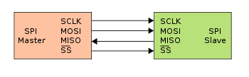
  • Master and Slave Devices:

    • SPI communication involves at least one master and one or more slave devices.
    • The master generates the clock signal and initiates data transfers.
  • Pin Configuration:

    • MISO (Master In Slave Out): Data sent from slave to master.
    • MOSI (Master Out Slave In): Data sent from master to slave.
    • SCLK (Serial Clock): Clock signal generated by the master.
    • SS (Slave Select): Signal used by the master to select the slave.
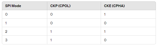
  • Clock Configuration:

    • The clock rate is derived from the system clock and can be adjusted to various frequencies.
    • Clock polarity (CKP) and phase (CKE) must be configured according to the slave device’s specifications.

SPI Modes:

The combination of clock polarity and phase results in four possible SPI modes:

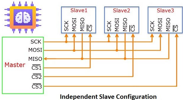
SPI Bus Configurations:

SPI devices can be connected in different configurations:

  • Daisy Chain: Devices are connected in a circular manner, passing data through each device until it reaches the destination. This configuration uses a single SS line for all devices, simplifying the connection.

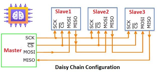
  • Independent Slave: Each slave has its own SS line, allowing the master to select each slave independently. This configuration can become impractical with many slaves due to the need for numerous IO pins.

Advantages of SPI:

  • Full-duplex communication.
  • High-speed data transfer rates.
  • Minimal wiring (typically 4 lines).
  • Simple hardware setup without the need for unique addresses for slaves.
  • Flexible data transfer sizes.

Diadvantages of SPI:

  • No hardware acknowledgment from slaves.
  • Typically supports only one master device.
  • Requires more pins compared to I2C.
  • No built-in error-checking.
  • Limited to short-distance communications.

Using SPI with Microcontrollers:

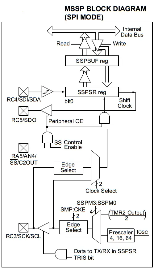
Microchip PIC microcontrollers come equipped with the Master Synchronous Serial Port (MSSP) module, which supports both Serial Peripheral Interface (SPI) and Inter-Integrated Circuit (I2C) modes. 

Pin Configuration

SPI allows for synchronous transmission and reception of 8-bit data frames using the following pins:

  • Serial Data Out (SDO): RC5/SDO
  • Serial Data In (SDI): RC4/SDI/SDA
  • Serial Clock (SCK): RC3/SCK/SCL
  • Slave Select (SS) (for Slave mode): RA5/AN4/SS/C2OU

Operation

To initialize SPI, configure control bits in the SSPCON and SSPSTAT registers:

  • To initialize SPI, configure control bits in the SSPCON and SSPSTAT registers:

    • Master Mode: Set SCK as the clock output.
    • Slave Mode: Set SCK as the clock input.
    • Configure the following settings:
      1. Clock Polarity (CKP)
      2. Clock Edge (CKE)
      3. Data Input Sample Phase (SMP)
      4. Clock Rate (in Master mode)
      5. Slave Select mode (in Slave mode)

The MSSP module contains a shift register (SSPSR) and a buffer register (SSPBUF). The system shifts data out with the Most Significant Bit (MSB) first, and it stores the received data in SSPBUF. The Buffer Full (BF) bit and the SSPIF interrupt flag indicate the status.

To enable the MSSP serial port, take the following actions:

  1. Set the SSPEN bit in SSPCON   
  2. Configure TRISx register bits:
    • SDI: Controlled by the SPI module
    • SDO: Clear TRISC<5>
    • SCK (Master mode): Clear TRISC<3>
    • SCK (Slave mode): Set TRISC<3>
    • SS: Set TRISC<4>

The MSSP module uses four registers in SPI mode:

  • SSPCON: Control register
  • SSPSTAT: Status register
  • SSPBUF: Data buffer register
  • SSPSR: Shift register (not directly accessible)

Master and Slave Modes

In Master mode, the SPI initiates data transfer when you write data to SSPBUF, which generates the SCK signal and shifts out the data. The maximum data transfer rate at 40 MHz reaches 10 Mbps.

In Slave mode, the device transmits and receives data using external clock pulses on SCK, with the SS pin providing synchronization. The device can also wake from Sleep mode upon receiving data.

Project Name: SPI Communication with PIC Microcontroller

This project demonstrates SPI (Serial Peripheral Interface) communication using a Microchip PIC microcontroller. Specifically, it involves setting up the MSSP (Master Synchronous Serial Port) module in SPI mode to transmit and receive data between the microcontroller and peripheral devices. The example showcases configuring two PIC microcontrollers for SPI communication, with one acting as the master and the other as the slave, highlighting the necessary steps and considerations for proper communication.

Code (in C using XC8 Compiler):

Configuring SPI Master:

To configure the PIC16F877A microcontroller as an SPI master, start by programming the SSPM3 bits in the SSPCON1 register to set the SPI mode and adjust the clock rate. Enable the synchronous serial port by setting the SSPEN bit. Next, configure clock behavior with the CKP and CKE bits and adjust the SMP bit for data sampling timing. Set the I/O pins: SDO as output, SDI as input, and SCK as output. Optionally, enable SPI reception interrupts and ensure PEIE and GIE bits are enabled. Finally, read the received data from the SSPBUF register while clearing the BF and SSPIF bits.

Initialization and Write Function

The code begins with configuration bits that set essential parameters for the PIC16F877A microcontroller, such as selecting a high-speed oscillator and disabling the watchdog timer for stable operation.

Next, it includes necessary header files and defines the clock frequency at 4 MHz. The I/O pins for user inputs—UP, Down, and Send—are defined, corresponding to the buttons connected to the microcontroller.

Following this, two function declarations are provided: SPI_Master_Init(), which initializes the SPI communication as a master, and SPI_Write(uint8_t), which sends data via SPI. This setup prepares the microcontroller for effective data communication with other SPI devices.

//Configuration bits
#pragma config FOSC = HS    // High-speed oscillator
#pragma config WDTE = OFF   // Watchdog Timer Enable (WDT disabled)
#pragma config PWRTE = OFF  // Power-up Timer Enable (PWRT disabled)
#pragma config BOREN = ON   // Brown-out Reset Enable (BOR enabled)
#pragma config LVP = OFF    // Low-Voltage (single-supply) In-Circuit Serial Programming Enable (LVP disabled)
#pragma config CPD = OFF    // Data EEPROM Memory Code Protection (Data EEPROM code protection off)
#pragma config WRT = OFF    // Flash Program Memory Write Enable (Write protection off)
#pragma config CP = OFF     // Flash Program Memory Code Protection (Code protection off)

#include <xc.h>
#include <stdint.h>
#include "config.h"
#define _XTAL_FREQ 4000000

// IO Pins Definitions
#define UP   RB0
#define Down RB1
#define Send RB2

// Function Declarations
void SPI_Master_Init();
void SPI_Write(uint8_t);

// Function Definitions
void SPI_Master_Init()
{
  // Set SPI Mode To Master + Set SCK Rate To Fosc/64
  SSPM0 = 0;
  SSPM1 = 0;
  SSPM2 = 0;
  SSPM3 = 0;
  // Enable The Synchronous Serial Port
  SSPEN = 1;
  // Configure Clock Polarity & Phase (SPI Mode Num. 1)
  CKP = 0;
  CKE = 0;
  // Configure Sampling Time (Middle)
  SMP = 0;
  // Configure IO Pins For SPI Master Mode
  TRISC5 = 0; // SDO -> Output
  TRISC4 = 1; // SDI -> Input
  TRISC3 = 0; // SCK -> Output
}

void SPI_Write(uint8_t Data)
{
  SSPBUF = Data; // Transfer Data To Buffer Register
}

Main Routine

This section of the code emphasizes the main program logic, which involves using push buttons to increment, decrement, and send a data value over SPI. Three buttons are connected to the microcontroller, each performing a specific action: increasing the data value, decreasing it, or sending it via SPI when pressed. The program continuously displays the data on an output port, allowing for real-time feedback. The program runs in an infinite loop, constantly checking the status of the buttons, updating the data value, and transmitting it when needed. This simple user interface allows interaction through physical buttons and feedback through visual output such as LEDs or a display.

// Main Routine
void main(void)
{
  // Peripherals & IO Configurations
  SPI_Master_Init(); // Initialize SPI as Master @ Fosc/64 SCK
  uint8_t Data = 0; // Data Byte
  TRISB = 0x07;     // RB0, RB1 & RB2: Input Pins (Push Buttons)
  TRISD = 0x00;     // Output Port (4-Pins)
  PORTD = 0x00;     // Initially OFF
  
  while(1)
  {
    // Increment Data Value
    if (UP)
    {
      Data++;
      __delay_ms(250);
    }
    // Decrement Data Value
    if (Down)
    {
      Data--;
      __delay_ms(250);
    }
    // Send Data Value Via SPI
    if (Send)
    {
      SPI_Write(Data);
      __delay_ms(250);
    }
    PORTD = Data; // Display Current Data Value @ PORTD
  }
  return;
}

Configuring SPI SLAVE:

To configure the PIC16F877A microcontroller as an SPI master, follow these steps: First, set the SPI mode to Master by programming the SSPM3 bits in the SSPCON1 register and adjusting the clock rate. Next, enable the synchronous serial port by setting the SSPEN bit. Then, configure the clock behavior by setting the CKP and CKE bits for polarity and phase. Adjust the SMP bit in the SSPSTAT register for data sampling timing. Set the I/O pins with SDO as output, SDI as input, and SCK as output. Optionally, enable SPI reception interrupts by setting the SSPIE bit in the PIE1 register and ensure PEIE and GIE bits are enabled. Finally, read received data from the SSPBUF register, clearing the BF and SSPIF bits afterward.

Code (in C using XC8 Compiler):

Configuration and Initialization

In the initial section, configuration settings define for the PIC16F877A microcontroller. This includes selecting the oscillator type, disabling the watchdog timer, and configuring the brown-out reset. These configuration directives play a crucial role in determining how the microcontroller behaves during operation.

// CONFIG
#pragma config FOSC = XT        // Oscillator Selection bits (XT oscillator)
#pragma config WDTE = OFF       // Watchdog Timer Enable bit (WDT disabled)
#pragma config PWRTE = OFF      // Power-up Timer Enable bit (PWRT disabled)
#pragma config BOREN = ON       // Brown-out Reset Enable bit (BOR enabled)
#pragma config LVP = OFF        // Low-Voltage (Single-Supply) In-Circuit Serial Programming Enable bit (RB3 is digital I/O, HV on MCLR must be used for programming)
#pragma config CPD = OFF        // Data EEPROM Memory Code Protection bit (Data EEPROM code protection off)
#pragma config WRT = OFF        // Flash Program Memory Write Enable bits (Write protection off; all program memory may be written to by EECON control)
#pragma config CP = OFF         // Flash Program Memory Code Protection bit (Code protection off)

// #pragma config statements should precede project file includes.
// Use project enums instead of #define for ON and OFF.

#include <xc.h>
#include <stdint.h>

// Function Prototypes
void SPI_Slave_Init(void);
uint8_t SPI_Read(void);

// Global Variable to Store Received Data
uint8_t Data; // Not recommended to use global variables for actual projects. Used here for demonstration purposes only.

Main Function and SPI Interrupt Handling

The second part of the code handles the main functionality, including the SPI communication and interrupt service routine. The interrupt service routine (ISR) is crucial for managing SPI data reception. When new data is received, indicated by the SSPIF flag, the ISR reads the data from the SSPBUF register and clears the interrupt flag to ensure smooth operation.

// Interrupt Service Routine
void __interrupt() ISR(void)
{
    if(SSPIF)
    {
        Data = SSPBUF;  // Read the received data from the buffer
        SSPIF = 0;      // Clear the interrupt flag
    }
}

// Main Function
void main(void)
{
    SPI_Slave_Init(); // Initialize SPI in slave mode
    TRISB = 0x00;     // Set PORTB as output to display received data

    while(1)
    {
        // Display the received data on PORTB
        PORTB = Data;
    }

    // Return statement included to avoid compilation warnings. Not required in practice due to infinite loop.
    return;
}

// Function to Initialize SPI in Slave Mode
void SPI_Slave_Init(void)
{
    // Set SPI mode to Slave with SS enabled
    SSPM0 = 0;
    SSPM1 = 0;
    SSPM2 = 1;
    SSPM3 = 0;

    // Enable the synchronous serial port
    SSPEN = 1;

    // Configure the clock polarity and phase (SPI Mode 1)
    CKP = 0;
    CKE = 0;

    // Clear the SMP bit
    SMP = 0;

    // Configure the I/O pins for SPI slave mode
    TRISC5 = 0; // SDO -> Output
    TRISC4 = 1; // SDI -> Input
    TRISC3 = 1; // SCK -> Input
    PCFG3 = 0;  // Set SS (RA5/AN4) to be digital I/O
    PCFG2 = 1;
    PCFG1 = 0;
    PCFG0 = 0;
    TRISA5 = 1; // SS -> Input

    // Enable SPI interrupt
    SSPIE = 1;
    PEIE = 1;
    GIE = 1;
}

// Function to Read Data from SPI Buffer
uint8_t SPI_Read(void)
{
    uint8_t data = 0;
    if(BF) // Check if any new data is received
    {
        data = SSPBUF;  // Read the buffer
        BF = 0;         // Clear the buffer-full indicator bit
        SSPIF = 0;      // Clear the interrupt flag bit
        SSPOV = 0;      // Clear the overflow indicator bit
    }
    return data;
}

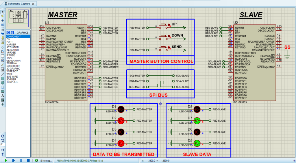
Proteus Configuration :

  • Open Proteus & Create New Project and click next

  • Click on Pick Device
  • Search for PIC16F877A & LED-RED & LED-GREEN & BUTTON
  • Click on Terminal Mode then choose (DEFAULT & POWER &GROUND)
  • finally make the circuit below and start the simulation
PIC16F877 SPI Proteus simulation circuit design with detailed wiring connections

That’s all!

If you have any questions or suggestions don’t hesitate to leave a comment below

You Might Also Like

Leave a Comment


Are you sure want to unlock this post?
Unlock left : 0
Are you sure want to cancel subscription?
-
00:00
00:00
Update Required Flash plugin
-
00:00
00:00