PIC16F877 Microcontroller I/O GPIO Ports Overview

by Marwen Maghrebi

In this article, we’ll explore the PIC16F877 Microcontroller I/O GPIO Ports, covering how to configure and use them effectively in your projects.

Things used in this project

Software apps and online services:

1- MPLAB

2- Proteus 8

Exploring PIC16F877 Microcontroller I/O GPIO Ports

This project delves into the PIC16F877 microcontroller, specifically its I/O GPIO ports, essential for interfacing with peripherals and sensors. We’ll break down the fundamental concepts behind Input/Output (I/O) ports and General Purpose Input/Output (GPIO) pins, which are key to interacting with external devices. Once you grasp how to configure and use these ports, you’ll gain the skills to expand your embedded systems’ capabilities.

Understanding GPIO Pins:

GPIO pins, short for General Purpose Input/Output pins, are the backbone of microcontroller operations. These pins enable versatile interfacing with external components, which is especially useful when working with PIC16F877 Microcontroller I/O GPIO Ports. In most cases, the pins on a microcontroller act as GPIOs, facilitating essential input/output operations.

Specialized Pins on the PIC16F877:

Apart from GPIO pins, the PIC16F877 has several specialized pins:

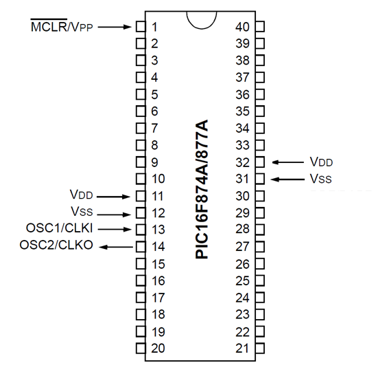
  • Power Supply pins: Vdd & Vss
  • Oscillator pins: OSC1 & OSC2, providingthe necessary clock input.
  • MCLR/VPP: Master Clear Reset pin,facilitating deliberate MCU restart.
  • VUSB: External USB power source pin.

Organizing GPIO Pins into Ports:

Typically, most microcontroller pins are organized into ports, as described in the PIC16F877A datasheet. Each port consists of multiple pins, often grouped into 8-bit ports, though this can vary across different microcontrollers.

For example, in the PIC16F877A:

  • PORTA: 6 pins (RA0 to RA5)
  • PORTB: 8 pins (RB0 to RB7)
  • PORTC: 8 pins
  • PORTD: 8 pins
  • PORTE: 3 pins (RE0 to RE2)

How Digital Input/Output Ports Operate:

Digital input/output ports in microcontrollers, including PORTB, are managed by two essential registers:

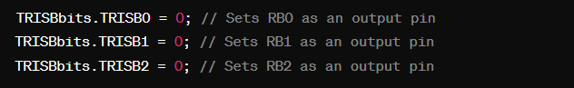
  • TRISx Register: This register determines whether each pin functions as an input or an output.
  • PORTx Register:This register is responsible for reading the state of input pins or setting the state of output pins.

For instance, with PORTA, you would use TRISA and PORTA; for PORTB, it would be TRISB and PORTB. The key actions involved in manipulating an I/O port include configuration and read/write operations.

Configuring I/O Pins:

To configure the PIC16F877 Microcontroller I/O GPIO Ports:

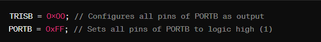
  • Setting a bit to 1 (High) in the TRISx register designates the corresponding pin as an input.
  • Setting a bit to 0 (Low) in the TRISx register designates the corresponding pin as an output.

To configure all pins of a port simultaneously, follow the same principles.

In C programming, several methods manipulate bits and registers, including:

  • Register Overwriting Method

  • Bit-Masking Method

  • Bit-Fields Method (recommended for XC8 users)

Reading and Writing Digital I/O Pins:

Once you’ve configured an I/O pin, you gain the ability to either read its state (if configured as an input) or alter its logical state (if configured as an output). The PORTx register serves as a linchpin in this process, with the value written to it dictating the logical state of the corresponding pins (High: 1/Low: 0).

Writing to PORTx Register:

When you write a 1 (High) to a bit of the PORTx register, you effectively set the corresponding pin to High. Conversely, writing a 0 (Low) to a bit of the PORTx register sets the corresponding pin to Low.

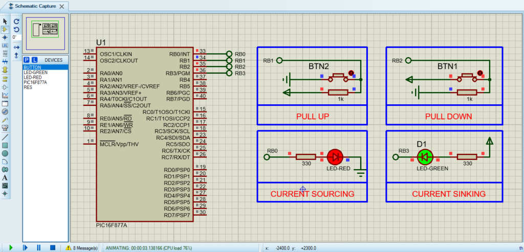
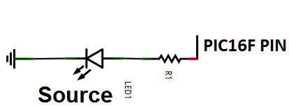
  • Output Pins Current Sourcing Configuration:

When configured in this manner, the output pin acts as a (+5v) source, supplying current to drive small loads (e.g., LEDs, Transistors, Relays, Optocouplers, etc.). A typical pin in our microcontroller can source up to 25 mA for each I/O pin.

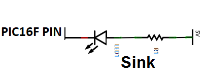
  • Output Pins Current Sinking Configuration:

Conversely, in the sinking configuration, the output pin functions as a (0v or Ground) sink, drawing current from small loads (e.g., LEDs, Transistors, Relays, Optocouplers, etc.). Similar to sourcing, a typical pin in our microcontroller can sink up to 25 mA for each I/O pin.

Reading Input Pins:

To read the logical state of an input pin accurately, additional hardware connections are necessary to ensure stable system behavior. Leaving an I/O pin unconnected while using it as an input should be avoided, as it leads to inconsistent input. To mitigate this, input pins are commonly pulled-up or pulled-down.

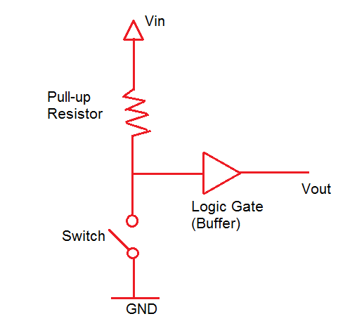
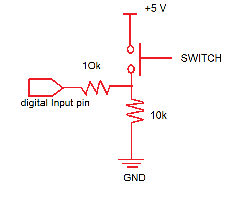
  • Input Pins Pull-Up Configuration:

In this configuration, the pin is consistently pulled-up to High (logic 1) until an event drives it Low (to 0). Typically, a 10kohm resistor is connected between the input pin and Vdd (+5v).

  • Input Pins Pull-Down Configuration:

Contrarily, in this setup, the pin is continuously pulled-down to Low (logic 0) until an event drives it High (to 1). Here, a 10kohm resistor is connected between the input pin and Vss (0v or Gnd).

Project: Controlling LEDs with Current Sourcing and Sinking Using PIC16F877A

The objective of this project is to control two LEDs using the PIC16F877A microcontroller, demonstrating both current sourcing and current sinking configurations. We’ll also use input pins with pull-up and pull-down resistors to control these LEDs.

Code (in C using XC8 Compiler):

Configuration Bits

The configuration bits control how the PIC16F877A microcontroller operates during startup and runtime. These settings are crucial for the microcontroller’s performance and ensure it functions properly for the specific project.

  • FOSC = XT: This setting selects the XT oscillator mode, which uses an external crystal for clock generation. In this project, an 8 MHz crystal is defined.
  • WDTE = OFF: The Watchdog Timer is disabled, meaning the microcontroller will not automatically reset if the program stalls.
  • PWRTE = OFF: Disables the Power-up Timer, which usually adds a delay during startup to stabilize power.
  • BOREN = ON: Enables Brown-out Reset, which resets the microcontroller if the voltage supply drops below a safe level.
  • LVP = OFF: Disables Low-Voltage Programming, freeing up the RB3 pin for digital I/O.
  • CPD, WRT, CP = OFF: These settings disable protection for EEPROM and program memory, allowing full access for code writing.
// Configuration Bits
#pragma config FOSC = XT        // Oscillator Selection bits (XT oscillator)
#pragma config WDTE = OFF       // Watchdog Timer Enable bit (WDT disabled)
#pragma config PWRTE = OFF      // Power-up Timer Enable bit (PWRT disabled)
#pragma config BOREN = ON       // Brown-out Reset Enable bit (BOR enabled)
#pragma config LVP = OFF        // Low-Voltage Programming Enable bit (RB3 is digital I/O, HV on MCLR must be used for programming)
#pragma config CPD = OFF        // Data EEPROM Memory Code Protection bit (Data EEPROM code protection off)
#pragma config WRT = OFF        // Flash Program Memory Write Enable bits (Write protection off; all program memory may be written to by EECON control)
#pragma config CP = OFF         // Flash Program Memory Code Protection bit (Code protection off)

Include and Define

The code begins by including the xc.h header file, which provides access to standard library functions for PIC microcontrollers. This allows the program to access specific registers and functions. Next, the code defines the crystal frequency using #define _XTAL_FREQ 8000000, which specifies the external clock frequency as 8 MHz. This value is used by the delay functions in the program to correctly time events like turning LEDs on and off.

// Include necessary libraries
#include <xc.h>

// Define crystal frequency
#define _XTAL_FREQ 8000000

Main Function

The main() function is the core of the program, where the microcontroller’s input and output pins are configured, and the logic for controlling the LEDs is implemented.

  • Pin Configuration: The pins connected to the LEDs and input switches are configured as either input or output. RB0 is set as an output for current sourcing (LED1), while RB3 is set as an output for current sinking (LED2). RB1 is set as an input with a pull-up resistor, and RB2 is set as an input with a pull-down resistor. This ensures proper behavior when checking input states.
  • Initial States: Before entering the main loop, the LEDs are initialized to be off. LED1 (RB0) is set to low, turning it off in the current sourcing configuration. LED2 (RB3) is set to high, turning it off in the current sinking configuration.
  • Main Program Loop: The loop constantly checks the state of the input pins (RB1 and RB2). If RB1 (pull-up) is low (button pressed), LED1 is turned on by setting RB0 to high. If RB2 (pull-down) is high (button pressed), LED2 is turned on by setting RB3 to low. This demonstrates controlling LEDs using current sourcing and sinking, and how pull-up and pull-down resistors affect input signal interpretation.
void main() {
    // Configure I/O pins
    TRISB0 = 0; // Set RB0 as output for current sourcing (LED1)
    TRISB3 = 0; // Set RB3 as output for current sinking (LED2)
    TRISB1 = 1; // Set RB1 as input with pull-up resistor
    TRISB2 = 1; // Set RB2 as input with pull-down resistor
    
    // Initialize outputs
    RB0 = 0; // Ensure LED1 is off initially
    RB3 = 1; // Ensure LED2 is off initially (active low configuration)
    
    // Main program loop
    while (1) {
        // Check state of RB1 (pull-up configuration)
        if (RB1 == 0) {
            RB0 = 1; // Turn on LED1 (current sourcing)
        } else {
            RB0 = 0; // Turn off LED1
        }
        
        // Check state of RB2 (pull-down configuration)
        if (RB2 == 1) {
            RB3 = 0; // Turn on LED2 (current sinking)
        } else {
            RB3 = 1; // Turn off LED2
        }
    }
}

Proteus Configuration :

  • Open Proteus & Create New Project and click next

  • Click on Pick Device
  • Search for STM32F103C6 & BUTTON & LED-RED & LED GREEN
  • Click on Terminal Mode then choose (DEFAULT & POWER &GROUND)
  • finally make the circuit below and start the simulation
PIC16F877 microcontroller circuit diagram in Proteus simulation with I/O GPIO ports configuration

That’s all!

If you have any questions or suggestions don’t hesitate to leave a comment below

You Might Also Like

Leave a Comment


Are you sure want to unlock this post?
Unlock left : 0
Are you sure want to cancel subscription?
-
00:00
00:00
Update Required Flash plugin
-
00:00
00:00